Announcement about MIT.nano, with video
http://newsoffice.mit.edu/2014/new-building-will-be-hub-for-nanoscale-research-0429
New building will be a hub for nanoscale research
“MIT.nano,” to be built in the heart of campus, will house advanced cleanroom, imaging, and prototyping facilities.
Watch Video
David L. Chandler | MIT News Office
April 29, 2014
Starting in 2018, researchers from across MIT will be able to take advantage of comprehensive facilities for nanoscale research in a new building to be constructed at the very heart of the Cambridge campus.
The 200,000-square-foot building, called “MIT.nano,” will house state-of-the-art cleanroom, imaging, and prototyping facilities supporting research with nanoscale materials and processes — in fields including energy, health, life sciences, quantum sciences, electronics, and manufacturing. An estimated 2,000 MIT researchers may ultimately make use of the building, says electrical engineering professor Vladimir Bulović, faculty lead on the MIT.nano project and associate dean for innovation in the School of Engineering.
“MIT.nano will sit at the heart of our campus, and it will be central to fulfilling MIT’s mission in research, education, and impact,” says MIT President L. Rafael Reif. “The capabilities it provides and the interdisciplinary community it inspires will keep MIT at the forefront of discovery and innovation, and give us the power to solve urgent global challenges. By following the lead of faculty and student interest, MIT has a long tradition of placing bold bets on strategic future technologies, and we expect MIT.nano to pay off in the same way, for MIT and for the world.”
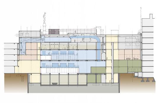
MIT.nano will house two interconnected floors of cleanroom laboratories containing fabrication spaces and materials growth laboratories, greatly expanding the Institute’s capacity for research involving components that are measured in billionths of a meter — a scale at which cleanliness is paramount, as even a single speck of dust vastly exceeds the nanoscale. The building will also include the “quietest” space on campus — a floor optimized for low vibration and minimal electromagnetic interference, dedicated to advanced imaging technologies — and a floor of teaching laboratory space. Finally, the facility will feature an innovative teaching and research space, known as a Computer-Aided Visualization Environment (CAVE), allowing high-resolution views of nanoscale features.
“The tools of nanotechnology will play a critical part in how many engineering disciplines solve the problems of the 21st century, and MIT.nano will shape the Institute’s role in these advances,” says Ian A. Waitz, dean of the School of Engineering and the Jerome C. Hunsaker Professor of Aeronautics and Astronautics. “This project represents one of the largest commitments to research in MIT’s history. MIT.nano will carry the last two decades of research into new realms of application and discovery.”
“Usually we talk about how science enables new technology, but discovery is a two-way street,” adds Maria Zuber, MIT’s vice president for research and the E.A. Griswold Professor of Geophysics. “In MIT.nano, technology will advance basic science through the extraordinary observations that will be possible in this state-of-the-art facility.”

